The electrical behaviour of transistors can be described more or less accurately by a number of equations relating the movement of the electrons in the semiconductor due to the applied potentials, and the resulting current flows. While this is useful for understanding transistor physics it is impractical for circuit design. Electrical models of the transistor behaviour have been devised that can be used in straightforward circuit analysis and design: these are equivalent circuit models, and the parameters of these models are the transistor parameters.
For circuit analysis by hand, the equivalent circuits are relatively simple. Generally they are divided into ‘DC’ models, for determining the steady bias conditions or operating point of the circuit, and small-signal models for determining the circuit response to an applied AC signal. Examples of such models for a bipolar junction transistor are the Ebers–Moll model, which is a DC model, and the hybrid-π model, which is a small-signal model (Figs. a, b). The transistor parameters in each model are the values for the equivalent-circuit components. For example, the parameters of the Ebers–Moll model are the current transfer ratios, αF and αR, and the saturation currents of the p-n junctions formed by the emitter-base and the collector-base junctions; the parameters of the hybrid-π model are the resistor and the capacitor values, and the transconductance.
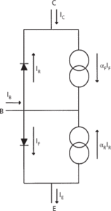
(a) Ebers–Moll DC model for a bipolar junction transistor
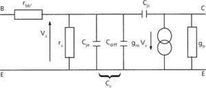
(b) Hybrid-π small-signal model for a bipolar transistor
Some small-signal models are derived from the two-port analysis of the transistor behaviour (see network). For example, the hybrid parameter model for a bipolar transistor in common-emitter configuration results in terms such as the input resistance hie, the output admittance hoe, and the forward-current gain hfe (gain parameter on the current-controlled current source at the output port). This hybrid parameter model is relatively archaic and should not be confused with the hybrid-π model of the bipolar transistor. The term hfe is often found in transistor data sheets, and can be identified with the forward-current gain β.
In practical devices the equivalent-circuit models can also include components to model the packages that the devices are placed in. This is particularly important at high frequencies where the packages can contribute significant capacitance and inductance that can strongly affect the overall electrical behaviour of the transistor.
When computer-aided design is used in the circuit analysis and design, more sophisticated equivalent-circuit models can be employed, making use of the computational power available to perform many more calculations than would be possible by hand. The SPICE model for a bipolar transistor is shown in Fig. c, and the associated parameter list is given in the table. Various levels of sophistication can be included in such models.
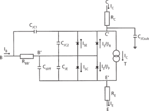
(c) SPICE model for bipolar transistor
Similar model approaches are employed for junction FETs and MOSFETs.
Model parameter
Default
Unit
Scaling
IS
saturation current
1E-16
amp
area
BF
ideal maximum forward current gain
100
NF
forward current ideality factor
1
VAF
forward Early voltage
∞
volt
IKF
corner for BF high-current roll-off
∞
amp
area
ISE
base-emitter leakage satn. current
0
amp
area
NE
base-emitter leakage ideality factor
1.5
BR
ideal maximum reverse current gain
1
NR
reverse current ideality factor
1
VAR
reverse Early voltage
∞
volt
IKR
corner for BR high-current roll-off
∞
amp
area
ISC
base-collector leakage satn. current
0
amp
area
NC
base-collector leakage ideality factor
2
RB
zero-bias (maximum) base resistance
0
ohm
1/area
RBM
minimum base resistance
RB
ohm
1/area
RE
emitter ohmic resistance
0
ohm
1/area
RC
collector ohmic resistance
0
ohm
1/area
CJE
base-emitter zero-bias junction cap.
0
farad
area
VJE
base-emitter built-in voltage
0.75
volt
MJE
base-emitter p-n doping grading
0.33
CJC
base-collector zero-bias junction cap.
0
farad
area
VJC
base-collector built-in voltage
0.75
volt
MJC
base-collector p-n doping grading
0.33
XCJC
fraction of Cbc connected internal to Rb
1
CJS
collector-substrate zero-bias junction cap.
0
farad
area
VJS
collector-substrate built-in voltage
0.75
volt
MJS
collector-substrate p-n doping grading
0
FC
forward-bias junction cap. coefficient
0.5
TF
forward transit time
0
sec
TR
reverse transit time
0
sec
EG
energy band gap
1.11
eV
KF
flicker noise coefficient
0
AF
flicker noise exponent
1
SPICE parameters for bipolar transistor (subset)
- interference fading
- interference figure
- interference filter
- interference pattern
- interference RNA
- interferogram
- interferometer
- interferometric synthetic aperture radar
- interferometry
- interferon
- interfingering
- inter finitum et infinitum non est pro-portio
- interflow
- interfluve
- intergalactic absorption
- intergalactic magnetic field
- intergalactic medium
- intergalactic space
- intergenerational equity
- intergenerational mobility
- intergenic suppressor
- interglacial
- Intergovernmental Panel on Climate Change
- intergrade
- intergranular