A crystalline solid, such as silicon or germanium, with an electrical conductivity (typically 105–10−7 siemens per metre) intermediate between that of a conductor (up to 109 S m−1) and an insulator (as low as 10−15 S m−1). As the atoms in a crystalline solid are close together, the orbitals of their electrons overlap and their individual energy levels are spread out into energy bands. Conduction occurs in semiconductors as the result of a net movement, under the influence of an electric field, of electrons in the conduction band and empty states, called holes, in the valence band. A hole behaves as if it was an electron with a positive charge. Electrons and holes are known as the charge carriers in a semiconductor. The type of charge carrier that predominates in a particular region or material is called the majority carrier and that with the lower concentration is the minority carrier. An intrinsic semiconductor is one in which the concentration of charge carriers is a characteristic of the material itself; electrons jump to the conduction band from the valence band as a result of thermal excitation, each electron that makes the jump leaving behind a hole in the valence band. Therefore, in an intrinsic semiconductor the charge carriers are equally divided between electrons and holes. In extrinsic semiconductors the type of conduction that predominates depends on the number and valence of the impurity atoms present. Germanium and silicon atoms have a valence of four. If impurity atoms with a valence of five, such as arsenic, antimony, or phosphorus, are added to the lattice, there will be an extra electron per atom available for conduction, i.e. one that is not required to pair with the four valence electrons of the germanium or silicon. Thus extrinsic semiconductors doped with atoms of valence five give rise to crystals with electrons as majority carriers, the so-called n-type conductors. Similarly, if the impurity atoms have a valence of three, such as boron, aluminium, indium, or gallium, one hole per atom is created by an unsatisfied bond. The majority carriers are therefore holes, i.e. p-type conductors.
Semiconductor devices have virtually replaced thermionic devices, because they are several orders of magnitude smaller, cheaper in energy consumption, and more reliable. The basic structure for electronic semiconductor devices is the semiconductor diode (see also transistor). This consists of a silicon crystal doped in such a way that half is p-type and half is n-type. At the junction between the two halves there is a depletion layer in which electrons from the n-type have filled holes from the p-type. This sets up a potential barrier, which tends to keep the remaining electrons in the n-region and the remaining holes in the p-region. However, if the p-region is biased with a positive potential, the height of the barrier is reduced; the diode is said to be forward biased, because the majority holes in the p-region can then flow to the n-region and majority electrons in the n-region flow to the p-region. When forward biased there is a good current flow across the barrier. On the other hand if the p-region is negatively biased, the height of the potential barrier is increased and there is only a small leakage current of minority electrons from the p-region able to flow to the n-region. Thus the p–n junction acts as an efficient rectifier, for which purpose it is widely used.
A crystalline solid with an electrical conductivity (typically 105–10−7 siemens per metre) intermediate between that of a conductor (up to 109 S m−1) and an insulator (as low as 10−15 S m−1). Semiconducting properties are a feature of metalloid elements, such as silicon and germanium. As the atoms in a crystalline solid are close together, the orbitals of their electrons overlap and their individual energy levels are spread out into energy bands. Conduction occurs in semiconductors as the result of a net movement, under the influence of an electric field, of electrons in the conduction band and empty states, called holes, in the valence band. A hole behaves as if it was an electron with a positive charge. Electrons and holes are known as the charge carriers in a semiconductor. The type of charge carrier that predominates in a particular region or material is called the majority carrier and that with the lower concentration is the minority carrier. An intrinsic semiconductor is one in which the concentration of charge carriers is a characteristic of the material itself; electrons jump to the conduction band from the valence band as a result of thermal excitation, each electron that makes the jump leaving behind a hole in the valence band. Therefore, in an intrinsic semiconductor the charge carriers are equally divided between electrons and holes. In extrinsic semiconductors the type of conduction that predominates depends on the number and valence of the impurity atoms present. Germanium and silicon atoms have a valence of four. If impurity atoms with a valence of five, such as arsenic, antimony, or phosphorus, are added to the lattice, there will be an extra electron per atom available for conduction, i.e. one that is not required to pair with the four valence electrons of the germanium or silicon. Thus extrinsic semiconductors doped with atoms of valence five give rise to crystals with electrons as majority carriers, the so-called n-type conductors. Similarly, if the impurity atoms have a valence of three, such as boron, aluminium, indium, or gallium, one hole per atom is created by an unsatisfied bond. The majority carriers are therefore holes, i.e. p-type conductors.
A material, such as silicon or germanium, whose electrical conductivity increases with temperature and is intermediate between metals and insulators. In pure semiconductors this effect is due to the thermal generation of equal numbers of negative charge carriers (electrons) and positive charge carriers (holes). These materials are called intrinsic or i-type semiconductors.
The introduction of specific types of impurity atoms into a pure semiconductor can significantly increase its conductivity: donor impurities, which belong to group 5 of the periodic table, greatly increase the number of conduction electrons and produce an n-type semiconductor; acceptor impurities, which belong to group 3, greatly increase the number of holes and produce a p-type semiconductor. These materials are called extrinsic semiconductors. The conductivity of an extrinsic semiconductor depends on the type and the amount (or doping level) of impurity present.
Semiconductors of different conductivity—n-type, p-type, highly doped n- and p-type, i-type—can be brought together to form a variety of junctions, which are the basis of semiconductor devices used as electronic components. The term semiconductor is frequently applied to the devices themselves.
A (usually) crystalline solid that in pure form exhibits a conductivity midway between that of metals and insulators, typically 1–1000 siemens per metre. A pure, or intrinsic semiconductor has an electron energy band structure of the form shown schematically in Fig. a. The valence band contains electrons that are used in bonding the atoms of the crystal together; at absolute zero of temperature (T = 0 K) this band is completely filled. The next highest allowed band of energies is the conduction band, which in semiconductors is separated from the valence band by an energy band gap of about one electronvolt. At absolute zero the conduction band is completely empty, and the material behaves like an insulator.
At room temperature (about 300 K), some electrons in the valence band gain enough thermal energy from their surroundings to cross the band gap and appear in the conduction band. The two bands are now partially filled and the possibility of electrical conduction exists; conduction is by electrons in the conduction band and holes in the valence band. The conductivity is still low compared to metals because of the relatively small numbers of carriers involved in conduction. The number density of electrons (n) in the conduction band equals the number density of holes (p) in the valence band, which in turn equals the intrinsic density (ni):
The Fermi energy level EF in an intrinsic semiconductor lies halfway between the conduction and valence band edges. The following expressions for n and p also hold:
Hence,
where Nc, Nv are the equivalent density of states in the conduction and valence bands, respectively, Eg is the energy gap, k the Boltzmann constant, and T the thermodynamic temperature. The intrinsic density, and hence conductivity, therefore has a strong temperature dependence.
The intrinsic conductivity is generally too low and too temperature dependent to be of practical use for electrical components. The carrier density can, however, be controlled by the careful introduction of donor and acceptor impurities into the semiconductor; this creates an extrinsic semiconductor. The impurities have the following specific properties.
A donor impurity
replaces a host atom in the crystal;
has one more valence electron than the atom it replaces;
after bonding into the crystal, the extra valence electron can be easily lost;
the free electron is in the conduction band, able to contribute to conduction;
the donor atom becomes a positive ion, a +ve charge fixed in place in the crystal.
An acceptor impurity
replaces a host atom in the crystal;
has one fewer valence electrons than the atom it replaces;
after bonding into the crystal, the vacant space is easily replaced by an electron from the valence band;
this leaves a hole in the valence band, able to contribute to conduction;
the acceptor atom becomes a negative ion, a –ve charge fixed in place in the crystal.
The addition of impurities to a semiconductor is known as doping. The impurity densities are chosen to be much greater than the intrinsic density, so that the temperature variation of carriers is overwhelmed, and the material conductivity is independent of temperature. The electron and hole densities in doped semiconductors are as follows:
In an n-type semiconductor:
donor density ND > acceptor density NA >> intrinsic density ni
electron density n = ND − NA, so electrons are majority carriers,
hole density p = ni%2/n, so holes are minority carriers,
the Fermi energy is in upper half of band gap.
In a p-type semiconductor:
acceptor density NA > donor density ND >> intrinsic density ni
hole density p = NA − ND, so holes are majority carriers,
electron density n = ni%2/p, so electrons are minority carriers,
the Fermi energy is in lower half of band gap.
At thermal equilibrium a dynamic equilibrium exists in a semiconductor. Mobile charges move around the crystal in a random manner due to scattering by the nuclei in the crystal lattice. The crystal retains overall charge neutrality and the number of charge carriers remains essentially constant. A continuous process of regeneration and recombination occurs, however, as thermally excited electrons enter the conduction band and other electrons return to the valence band and there combine with holes (see also recombination processes).
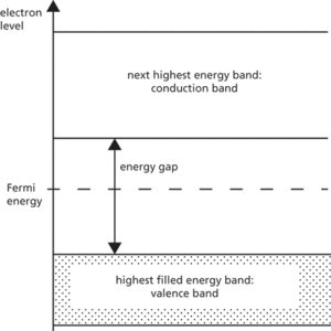
Energy band diagram of an intrinsic semiconductor
If an electric field is applied to the semiconductor, charge carriers move under the influence of the field but still undergo scattering processes. The result of the field is to impose a drift in one direction onto the random motion of the carriers (see also drift mobility; continuity equation).
Extrinsic semiconductors are used for making diodes, transistors, and integrated circuits (see also p-n junction; metal-semiconductor contact). The most common semiconductor material is silicon, which is used for around 99% of commercial semiconductor products. Compound semiconductors, such as gallium arsenide, are used in specialist applications such as microwave devices and optoelectronics.
http://electronics.howstuffworks.com/diode.htm ‘How Semiconductors Work’, on the howstuffworks website
https://www.doitpoms.ac.uk/tlplib/semiconductors/index.php An introduction to semiconductors, from the University of Cambridge
- chemoautotroph
- chemocline
- chemofossil
- chemoheterotroph
- chemoinformatics
- chemokine
- chemoreceptor
- chemostat cultivation
- chemostratigraphy
- chemosymbiosis
- chemosynthesis
- chemosystematics
- chemotaxis
- chemotaxonomy
- chemotherapy
- chemotropism
- ChemSketch
- Cheng Hao (1032–85)
- Cheng Ho
- Chengjiang fossils
- chenier
- chenier plain
- Chen’s theorem
- Cheollian-1
- CHEOPS