See integrated circuit.
A type of integrated circuit based on MOSFETs. MOS circuits have several advantages compared to bipolar integrated circuits for many low-frequency applications, and account for the majority of all semiconductor devices produced.
MOSFETs are self-isolating and no area-consuming isolation diffusions are required; this enables a very high functional packing density to be obtained. MOSFETs may be used as active load devices and a separate process is not therefore required to form resistors. When used as load devices pulse operation of the circuit is easily achieved using the gate electrodes to activate the device: power dissipation is greatly reduced, involving less complicated heating problems. A characteristic of MOSFETs is their exceptionally high input impedance. This allows the gate electrodes to be used as temporary storage capacitors thus keeping the circuits comparatively simple. This is called dynamic operation. Usually these circuits operate above a minimum specified frequency.
The relatively few processing steps required in manufacture, compared to bipolar integrated circuits, enables large chips to be made thus further increasing the functional compactness and reducing the costs. MOS integrated circuits tend however to be slower than their bipolar counterparts due to their inherently lower transconductance and to the fact that their speed is extremely dependent on the load capacitance.
Modern MOS ICs are made using a self-aligned gate process. In the self-aligned gate circuit the gate electrodes are formed before the source/drain diffusions are made; the most widely used method is known as the silicon gate technology (see diagram). Openings are made in the initial thick oxide layer and a thin layer of oxide grown to form the gate insulators. This is immediately covered with a layer of polycrystalline silicon (polysilicon) using a vapour-phase reaction. The polysilicon is then etched to form the gate electrodes together with some interconnections. The gate oxide is then removed from the regions not covered with polysilicon leaving openings through which the source/drain diffusions are made. The edges of these diffused regions are defined by the previously etched gate regions thus providing the required precision of alignment. The diffusing material also enters the polysilicon regions and dopes them, which has the desirable effect of reducing their resistivity. The whole wafer is covered with a further oxide layer, contact windows etched, and a metal layer is deposited and etched to form the interconnections. Several layers of metal interconnections are possible using this technique.
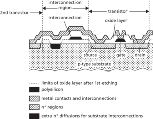
MOS integrated circuit: cross section of n-channel self-aligned circuit