MOS circuits or transistors that are fabricated using the V-groove technique. Regions of the required conductivity type are formed in (100) orientation silicon crystals using a combination of planar diffusion and epitaxy. V-groove etching is then performed, and the gate electrode formed in the groove, in order to produce vertical MOSFET transistors of the same structure as DMOS. This technique is used to produce MOS devices of very precise channel length; as with DMOS the channel length is determined by the diffusion rather than by photolithography. VMOS devices also contain an n− drift region (DMOS) in order to prevent punch-through. The length of the drift region determines the breakdown voltage of the device, as with DMOS devices, and the structure shown in Fig. a is used to form discrete high-power MOSFETs. Operating voltages of about 300 volts can be achieved using a drift length of about 25 micrometres although voltages of about 100 V are more usual. The ‘on’ impedance can be kept low (of the order of a few ohms) using several long grooves on each transistor chip.
The technique is also used to produce an array of transistors for applications, such as ROM (read-only memory), that are used with a common source (Fig. b). In this case the device is physically inverted and the groove must be taken right through to the substrate. The drift region can therefore only be about two micrometres in length in order to accommodate the gate electrodes. An inverted VMOS circuit is only suitable for low-power high-speed applications up to microwave frequencies. It has however an increased functional packing density compared to DMOS.
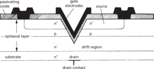
(a) VMOS power transistor
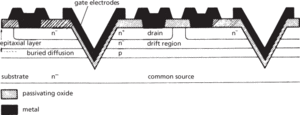
(b) Common-source VMOS
- Ground Communications Facilities
- ground control
- ground-control point
- ground crew
- ground current
- ground data
- ground data system
- grounded-base connection
- grounded-collector connection
- grounded-emitter connection
- grounded theory
- ground electrode
- ground failure
- ground frost
- ground ice
- ground information
- groundmass
- ground meristem
- ground moraine
- groundnut
- ground-penetrating radar
- ground plane
- ground potential
- ground range
- ground ray