See TTL.
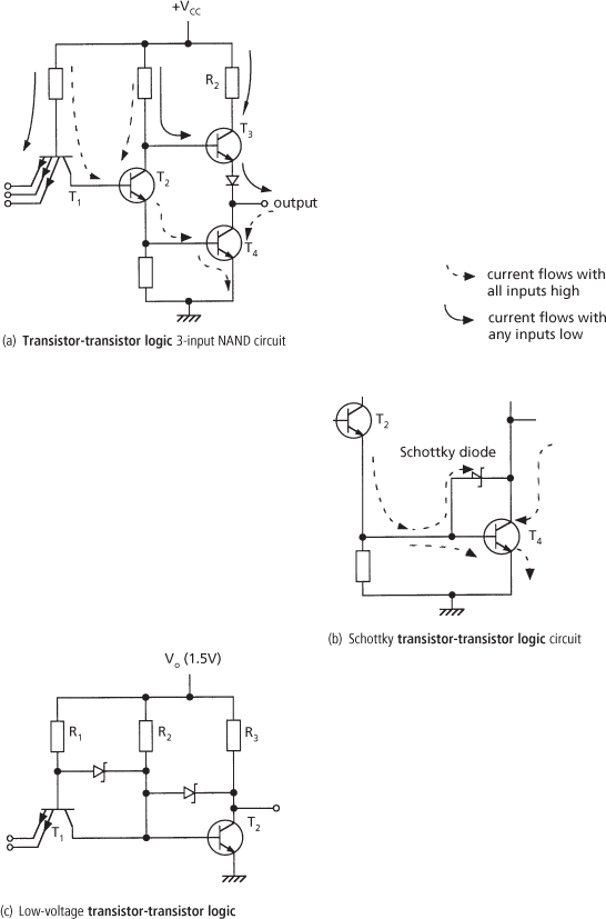
A family of high-speed integrated logic circuits in which the input is through a multiple-emitter bipolar junction transistor; usually the output stage is push-pull. Diode-transistor logic operates in a similar manner but the input is through a number of diodes. A typical circuit (a three input NAND circuit) is shown in Fig. a. If the input levels are all high, the emitter-base junctions of the input transistor T1 will all be reverse biased: current through the base will flow across the forward-biased collector junction to the phase-splitting transistor T2, which will switch on. Current flows through T2 to T4 and turns on T4. T3 will remain off as current is shunted away from the base and the output voltage will be low. If any one or more of the inputs is low, the emitter-base junction of T1 will be forward biased and current flows out of the base through the emitter of T1. The current is therefore diverted away from T2, and T2 and T4 will be turned off. The current through R2 flows into the base of T3 and T3 is switched on and the output voltage is high. The output voltage will change rapidly when the input conditions change since the transistors drive the level in both directions.

The biggest limitation in speed is caused by the delay time due to hole storage in the saturated output transistor T4. The speed may be improved by adding a Schottky diode with low diode forward voltage across the base-collector junction of T4. This circuit is called Schottky TTL and part of the circuit is shown in Fig. b. This diode prevents T4 saturating. Hole storage therefore does not occur in the collector-base junction and since it does not occur in Schottky diodes, T4 will be turned off very rapidly when the base current is cut off.
TTL circuits based around a standard power voltage of 5V were the most widely used form of TTL for digital circuit design, particularly in medium-scale integration (MSI) circuits, and for the glue logic that connected microprocessors to memory and input/output devices. Simplified low-voltage versions of TTL that are more suitable for large-scale integration (LSI) have also been produced. One such circuit is shown in Fig. c. Schottky diodes clamp the base-collector voltages across T1 and T2 and control the level of saturation. R2 is an additional resistor that allows the gate to operate from a supply voltage less than or equal to 1.5 volts.
TTL is also characterized by medium power dissipation and fan-out and good immunity to noise. TTL circuits may have high operating speeds but at the expense of power dissipation, since the higher the speed the greater the power consumed. They are also medium-scale integration (MSI) circuits. They are therefore not suitable for applications where low power dissipation and large functional packing density is required. MOS logic circuits are usually the circuits of choice for such applications but they operate at much lower speeds. CMOS circuits, in particular, have very low power dissipation and CMOS versions of TTL gates have been produced. More recently, CMOS has effectively supplanted TTL for most digital circuit applications.
- spider
- spider diagram
- spidering
- spider monkey
- spider plot
- spiders
- spiegel
- spigot
- Ingold, Sir Christopher Kelk (1893–1970)
- ingot
- Ingram, Vernon Martin
- INGRES
- ingress flight
- ingress–egress platform
- ingress–egress side hatch
- ingrown meander
- inguinal
- inhabited
- inhalation
- inherent addressing
- inherently ambiguous language
- inherently safe
- inherent moisture
- inherent weakness failure
- inheritance