See junction.
The region at which two semiconductors of opposite polarity meet, i.e. at which a p-type and n-type semiconductor meet. A simple p-n junction is formed from the same material in which approximately equal doping levels lead to two different conductivity types; this is known as a homojunction. A heterojunction is formed from two dissimilar materials. The properties of p-n junctions are used in many semiconductor devices, such as diodes and transistors.
The simplified energy diagrams of an unbiased junction, a forward-biased junction (positive voltage applied to the p-region), and a reverse-biased junction are shown in Fig. a. In the unbiased state equilibrium considerations demand that the Fermi level, EF (see energy bands), is constant throughout the bulk of the material. This causes distortion of the energy bands at the junction and results in an electric field across the junction. This field is known as the built-in field. At equilibrium there is a small depletion layer containing fixed ionized atoms and substantially no mobile charge carriers.
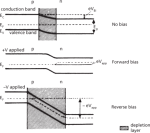
(a) Energy diagrams of a p-n junction (a homojunction)
Under reverse-bias conditions the depletion layer is increased as is the electric field across the junction, which thus acts as a barrier to current flow. Thermally generated charge carriers diffusing into the depletion layer are swept across the junction by the electric field and thus produce a small reverse saturation current, Io.
Under forward-bias conditions the built-in field virtually disappears and charge carriers are attracted across the junction into the opposite polarity type (where they become minority carriers) and cause a current to flow in an external circuit.
The current-voltage relationship of an ideal p-n homojunction under forward-bias conditions obeys an exponential relationship:
where e is the electronic charge, V the applied voltage, k the Boltzmann constant, and T the thermodynamic temperature. This is the Shockley equation (or ideal diode equation) and assumes that the current is due to the diffusion of charge carriers across the junction, that the injected minority carrier density is small compared to the majority carrier density, and that there is no generation or recombination of charge carriers in the depletion region. In practice these conditions are not always fulfilled, particularly in silicon where the intrinsic carrier concentration is low, and it is found that the Shockley equation may be modified so that the term eV/kT is replaced by eV/nkT, where n has a value between one and two.
The characteristic curve of a p-n junction depends on the geometry, the bias conditions, and the doping level on each side of the junction. A typical characteristic curve for a p-n junction diode is shown in Fig. b. Applications of simple p-n junctions include rectification, voltage regulation, and use as a varistor or varactor and as a switch.
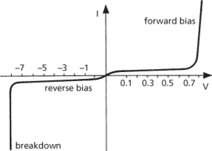
(b) Current-voltage characteristic of a p-n junction
- testis-determining factor
- test oracle
- testosterone
- test pattern
- test run
- test separator
- test statistic
- test suite
- test–retest reliability
- tetanus
- tether
- tethered satellite system
- Tethyan realm
- Tethys
- Tethys Sea
- Tet Offensive (29 January–25 February 1968)
- tetra-
- tetrachloroethene
- tetrachloromethane
- tetrachoric correlation coefficient
- Tetracorallia
- tetracorals
- tetracosactide
- tetracyanoquinodimethane
- tetrad