A technique used during the manufacture of LSI MOS integrated circuits and some forms of LSI bipolar integrated circuits, such as I2L. Regions of relatively thick silicon dioxide are used in order to isolate device areas. The coplanar process was developed in order to minimize the vertical projection of the oxide layer. A layer of silicon nitride is deposited on the surface of the silicon wafer and is etched to expose the regions of the surface where thick oxide is required. As oxidation takes place, the effective silicon surface moves downwards and is replaced by a thicker layer of silicon dioxide, so that approximately one third of the oxide is below the original exposed surface level (Fig. a). Oxidation may be preceded by etching of the exposed silicon surface so that the final oxide surface is at the same level as the original substrate (Fig. b). The silicon nitride is then removed from the rest of the surface and the integrated circuits are formed using normal planar-process technology.
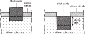
(a) Coplanar process with nitride etch (b) Nitride plus silicon etch
- byssate
- byssus
- byte
- byte-addressable
- byte code
- byte-order mark
- bytownite
- Byurakan Astrophysical Observatory
- Byzantine empire
- Byzantine Generals problem
- Byzantium
- BZ
- b-zone
- Bábism
- Bárány, Robert
- Békésy, Georg von
- Bénard cell
- Bézier curve
- Bézier patch
- Bézier surface
- Bézout’s lemma
- Bézout’s theorem
- Böserup model
- Bølling
- Bølling-Allerød interstadial