A logic circuit constructed in a MOS integrated circuit. It consists of a combination of MOSFETs in series or in parallel that perform the logic functions, i.e. act as AND or OR gates, etc. (Fig. a), coupled to other MOSFETs that determine the output voltages of the circuit. MOS logic circuits are classified according to the method of determining the output voltage, i.e. into ratio or ratioless circuits. The logic gates effectively act as switches when used with a suitable choice of high and low logic levels. When the required input conditions are fulfilled the combination switch is ‘on’ and provides a conducting path. If the switch is ‘off’ the gate does not conduct. The high logic level is chosen to be greater than the threshold voltage, VT, of the MOSFET; the low level is lower.
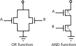
(a) MOS logic circuits
In a ratio circuit the logic gate, represented as a single switch transistor, TS, is connected in series with a load transistor TL. The drain of the load transistor is connected to the power supply and the source of the switch transistor to earth (Fig. b). The output is taken from the node, A, between the transistors. The circuit will usually be driving similar MOS logic gates. These have a very high input impedance. A voltage of magnitude greater than or equal to the drain voltage, VDD, is applied to the gate of TL. In static operation the voltage is applied continuously; in dynamic operation the voltage is applied on the application of a clock pulse in order to reduce dissipation.
A low logic level input to the gate of the switch transistor TS results in TS being ‘off’; CL is then charged by TL until the output voltage, VA, reaches a value sufficient to cause TL to turn off, i.e. until VA reaches (VGG – VT) or VDD, whichever is lower. Application of a high logic level to the gate of TS causes TS to be ‘on’ and CL discharges through TS. The output voltage VA falls to a level determined by the relative impedances of the two transistors.
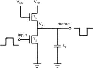
(b) Ratio circuit
It can be shown that the voltage VA at the node depends on the ratio of the aspect ratios of the devices, and these are manufactured to ensure an output voltage suitable for a low logic level, i.e. less than the threshold voltage of the following gate. The circuit provides inversion of the logic function; thus an AND function in TS provides a NAND output, etc.
If the dynamic version of the circuit (with the gate voltage of the load transistor clocked) is used a minimum rate of clocking must be specified to prevent loss of information at the output due to leakage paths causing the charge on the load capacitor to decay.
In a ratioless circuit (Fig. c) a second load transistor, T2, is connected in series between the first load transistor T1 and the logic gate, represented by a single switch transistor TS; the output voltage VB is taken from the node, B, between T1 and T2. A clocking system is employed, usually a four-phase system, to apply a bias to the gates of the load transistors T1 and T2 in turn. During phase one (ϕ1) bias is applied to the gate of T1, T1 is turned on, and the load capacitor CL (usually the gate of the switch transistor of the following stage) is charged to (VGG − VT). During phase two (ϕ2) bias is applied not to T1 but to the gate of T2. If a high logic level is applied to TS at this time, both T2 and TS will be turned on, CL will discharge through them, and the output voltage VB will fall to the low logic level. If TS is not turned on, i.e. a low logic level is applied to the gate of TS during ϕ2, CL will not discharge since no conducting path to earth exists and VB will remain at the high logic level. The output of the circuit is sampled by the following circuit during phases ϕ3 and ϕ4; information may thus only be supplied to TS once in every four clock phases.
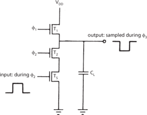
(c) Ratioless circuit
Operation of this circuit does not depend on the impedances of the devices and it is therefore termed ratioless. Power dissipation is very low since no conducting path ever exists directly between the power supply and earth and the circuits depend solely on charge storage in the load capacitance. The circuit is inverting and two gates are frequently combined to provide a noninverting circuit. If used in a dynamic shift register, for example, six transistors are needed for each bit of information.
A CMOS logic circuit uses complementary MOS transistors to provide the basic logic functions. The basic NAND gate is shown in Fig. d. CMOS circuits have the advantage that the power required is extremely low and they are suitable for applications where very little power consumption is a condition. They have a lower packing density than ratio circuits since every transistor requires its complement and therefore isolation of p-channel devices from n-channel devices is required. For convenience, groups of n-channel devices (and p-channel devices) are formed in the same area of the chip. The speed of operation is relatively slow, compared to transistor-transistor logic, because of the relatively large bulk capacitance of the substrate. CMOS circuits are however very resistant to stray noise pulses. Faster versions of CMOS circuits have been designed; the fastest version is the silicon-on-sapphire type of circuit (see silicon-on-insulator).
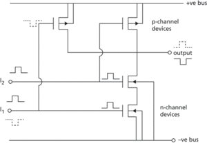
(d) CMOS NAND gate
- lee wave
- lee waves
- Lee, Yuan Tseh
- Lee–Kesler equation of state
- Lee’s disc
- left
- left and right derivative
- left-hand rule
- Left((in politics))
- left inverse
- left lateral fault
- left-linear grammar
- left shift
- left subtree
- left-to-right precedence
- left‐handed system
- legacy applications
- legacy networks
- legal disclaimer
- legal geography
- legalism
- legal positivism
- legal realism
- legal tender
- Legendre, Adrien-Marie (1752–1833)