A type of field-effect transistor that has an insulating layer of oxide, usually silicon dioxide, separating the gate from the drain-source conduction channel in the semiconductor. In an NMOS the channel is formed between n-type source and drain by negative charge carriers (i.e. electrons). In a PMOS the channel is formed between p-type source and drain by positive charge carriers (i.e. holes).
MOSFETs require no gate input current, other than a pulse to charge or discharge their input capacitance. They can operate at higher switching speeds and lower currents than bipolar transistors.
A field-effect transistor that uses the MOS capacitor as the basis of operation. The structure is shown in the diagram. The inversion layer forms a conducting bridge or channel between two electrodes – source and drain; the gate forms the third electrode. (For details of the electrical behaviour, see field-effect transistor.)
Both p-channel and n-channel MOSFET technologies are available, known as PMOS and NMOS respectively. Depletion-mode and enhancement-mode transistors can be made in both technologies. PMOS was the first MOSFET technology to be realized practically, followed by NMOS, which offered higher switching speeds for digital logic circuits. Both PMOS and NMOS technologies are combined on a single silicon wafer in one technology, called complementary MOS or CMOS. This offers lower power consumption than other MOS technologies, since power is consumed only during the logic switching cycle and not in static conditions. MOS technologies are used in the largest microprocessor and memory ICs. See also CMOS sensor.
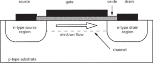
n-channel MOSFET structure
- tourmalinization
- Tournaisian
- tournament
- tournament method
- tourney
- tourquoise
- Touré, Sékou (1922–84)
- Toussaint L’Ouverture, François-Dominique (1743–1803)
- Toutatis
- tower
- Bayes ratio
- Bayes, Reverend Thomas (1701–61)
- Bayes's theorem
- Bayes theorem
- Bayes, Thomas (1702–61)
- Bayes’s theorem
- Bayes’ Theorem
- Bayes’ theorem
- Bayeux Tapestry
- Bayezid I (1347–1403)
- Bayezid II (c.1447–1512)
- bayhead barrier
- bayhead beach
- Bayle, Pierre (1647–1706)
- Bayle's trilemma