A two-terminal capacitor structure made in silicon technology: the top electrode – the gate – is a metal contact, the insulating or dielectric layer is silicon dioxide, and the counter electrode is provided by the silicon itself. An example of this structure for an n-channel capacitor is shown in Fig. a.
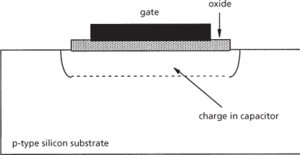
(a) n-channel MOS capacitor structure
The electrical behaviour of the MOS capacitor is governed by the behaviour of the silicon beneath the oxide layer, and can be described by four modes of operation: flat band, accumulation, depletion, and inversion; the schematic electron energy band diagrams for these operation modes are shown in Fig. b.
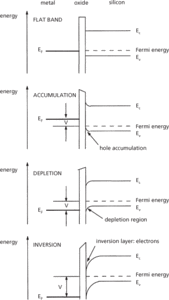
(b) Energy band structures for the n-channel MOS capacitor in four operation modes
In flat-band operation mode, the Fermi levels EF in the metal and the silicon are in alignment so the energy bands are completely flat. This is an equilibrium situation, and is defined as a reference point in MOS structures.
In accumulation mode, a negative voltage is applied to the metal, attracting free holes in the silicon to the surface beneath the oxide. There is a greater density of holes at the surface than the equilibrium p-type doping density, so there is effectively an accumulation of holes at the surface. The energy bands are bent upwards at the silicon surface, indicating higher hole density than deep in the silicon.
In depletion mode, a positive voltage is applied to the metal, repelling free holes from the silicon surface beneath the oxide. The hole density is now less than the equilibrium doping density, and the region beneath the oxide is depleted of charge carriers. The energy bands are bent downwards at the silicon surface, indicating lower hole density.
In inversion mode, a further positive voltage is applied to the metal, causing the energy bands to bend further downwards. At some value of applied voltage, the energy bands will bend sufficiently for the Fermi levels at the surface to move closer to the conduction band edge, indicating that in this region there is a higher density of electrons than holes: the surface layer appears n-type. The surface region is said to be inverted. This is the normal region of operation for MOSFETS. The inversion layer of electrons forms the counter electrode to the metal in what is effectively a parallel-plate capacitor structure. The variation of capacitance C with applied voltage V is shown in Fig. c.
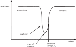
(c) Variation of capacitance with applied voltage for a MOS capacitor
- cycloaddition
- cycloalkanes
- cyclobutadiene
- cyclogenesis
- cyclohexadiene-1,4-dione
- cyclohexane
- cycloid
- cyclolysis
- cyclomatic number
- cyclomorphosis
- cyclone
- Cyclone Global Navigation Satellite System
- cyclone separator
- cyclone wave
- cyclonite
- cyclo-octatetraene
- cyclo-oxygenase
- cyclopean concrete
- cyclopel
- cyclopentadiene
- cyclopentadienyl ion
- cyclophane
- cyclopropane
- cyclopsam
- cyclosarin