A plated hole used to provide low-inductance connections on an integrated circuit. A via may be formed through the dielectric layer on the top of a wafer to interconnect two metallization patterns. A via may also be formed though the back of a wafer containing FETs where a low-inductance earth is required; this is especially useful for microwave or power FETs, and metal plating is used on the back of the wafer to provide a heat sink and earth plane simultaneously (see diagram).
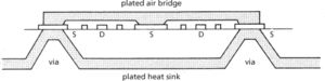
Vias formed through the back of a wafer
- double-dip recession
- double displacement
- double-dividend hypothesis
- Double Double
- double drift device
- double dummy
- double effect, principle of
- double-ended
- double entry bookkeeping
- double exponential distribution
- double factorial
- double fertilization
- double helix
- double image
- double integral
- double layer
- double-length arithmetic
- double-lined binary
- double-mindedness
- double-mode variable
- double modulation
- double negation
- double negation translation
- double planation
- double point