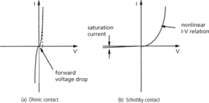
An intimate contact between a deposited metal and the underlying semiconductor, used to make electrical contact between the solid-state electronic device and the external circuit. The metal-semiconductor contact can be either low-resistance, often termed an ohmic contact, or a rectifying contact known as a Schottky barrier. The difference is in principle due to the relative energy difference between the Fermi levels in the metal and semiconductor. For an ohmic contact the Fermi levels should be in alignment, or their positions should be such that an accumulation of majority carriers is created at the surface of the semiconductor; this is shown in Fig. a for a metal-to-n-type semiconductor. For a Schottky-barrier contact the Fermi levels are not in alignment, causing a depletion of charge carriers at the surface of the semiconductor, shown in Fig. b, again for a metal-to-n-type semiconductor. This produces a potential barrier that the carriers must overcome in order for current to flow. The current-voltage relationship for a Schottky barrier is therefore very similar to that of a p-n junction, except that only majority carriers are considered.
Metal-semiconductor contact
Many practical semiconductors, such as silicon or gallium arsenide, possess defect states at the surface of the crystal: these can be thought of as unsatisfied interatomic bonds. These surface states readily fill with electrons from the conduction band of the semiconductor, and cause a depletion region to form at the surface in n-type semiconductors, even in the absence of a metal. Thus there already exists a potential barrier. The deposition of a metal produces only a small change to this barrier height. Obtaining a rectifying or Schottky contact is therefore reasonably straightforward. To produce an ohmic contact, the surface region of the semiconductor must be very heavily doped so that the resulting depletion region is narrow enough for conduction by field emission, or tunnelling, to take place. The resulting current-voltage relation is not linear – i.e. not ohmic – but produces only a small voltage drop. The heavy doping is generally provided by the contact metallization: this is often an alloy, a component of which is a dopant for the underlying semiconductor. During the heat treatment that is part of the contact formation, the dopants diffuse into the surface of the semiconductor to form the highly doped region for the ohmic contact.
- Tukey’s mean-difference plot
- tulip
- Tullgren funnel
- Tully–Fisher relation
- tumbleweed
- tumour
- tumour necrosis factor
- tumour-suppressor gene
- tumulus
- tunable magnetron
- tundish
- tundra
- Tundra Soil
- tundra soil
- tuneable laser
- tuned amplifier
- tuned circuit
- tuner
- Tung Chung-shu (c.179–c.104)
- tungstates
- tungsten
- tungsten carbide
- tungsten(symbol: W)
- Tunguska event
- tunicates