A bipolar junction transistor that has three terminals and one junction (Fig. a). The device consists of a bar of lightly doped (high-resistivity) semiconductor, usually n-type, with an opposite-polarity region of highly doped (low-resistivity) material located near the centre of the bar. Ohmic contacts are formed to each end of the bar (base 1 and base 2) and to the central region (emitter). Originally the emitter region was alloyed into the bulk material but planar diffused or planar epitaxial structures are now produced.
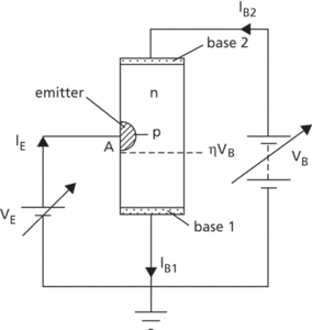
(a) Unijunction transistor
Under normal operating conditions base 1 is earthed and a positive bias, VB, applied to base 2. A point A on the least positive side of the emitter junction is considered. The voltage on the n side of the junction at point A is given by ηVB, where η is the intrinsic stand-off ratio:
RB1 is the resistance between point A and base 1 and RBB the resistance between base 1 and base 2.
If the voltage, VE, applied to the emitter is less than ηVB the junction is reverse biased and only a small reverse saturation current flows. If VE is increased above ηVB the junction becomes forward biased at point A and holes are injected into the bar. The electric field within the bar causes the holes to move towards base 1 and increase the conductivity in the region between point A and base 1. Point A becomes less positive and therefore more of the junction becomes forward biased; this causes the emitter current, IE, to increase rapidly. As IE increases the increased conductivity causes the emitter voltage to drop and the device exhibits a negative-resistance portion of the current-voltage characteristic (Fig. b).
The emitter voltage at which the device starts to conduct, Vp, is known as the peak point. At voltage Vv, known as the valley point, the device ceases to exhibit negative resistance. The switching time between the peak point and the valley point depends on the device geometry and the biasing voltage, VB, applied to base 2. It has been found to be proportional to the distance between point A and base 1.
If base 2 is open circuit, the I-V curve is essentially that of a simple p-n junction (Fig. c). As VB is increased the peak point, Vp, and the current, Iv, of the valley point also increase. The characteristics show little temperature dependence.
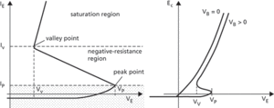
(b) Part of emitter I-V characteristic (c) Emitter I-V characteristics
The most common application of the unijunction transistor is in relaxation oscillator circuits.
- electro-optical effect
- electro-optical shutter
- electro-optics
- electroorganic reaction
- electro-osmosis
- electroosmosis
- electroosmotic mobility
- electropherogram
- P/O ratio
- porcelain jasper
- porcellanite
- Porco, Carolyn C. (1953– )
- porcupine
- pore
- pore fluid pressure
- pore space
- pore-water pressure
- Porifera
- porin
- pornography
- porosity
- porosity and permeability determination
- porous silicon
- porphyrin
- porphyritic