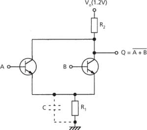
A family of integrated logic circuits that operates at a high speed at relatively low power. The basic NTL gate is shown in the diagram. It may be considered as a mixture of resistor-transistor logic (RTL) and a simplified form of emitter-coupled logic (ECL). The input transistors A and B form a long-tailed pair with resistor R1. The voltage gain is determined by the ratio R2/R1 and is adjusted to be slightly more than unity. Unlike other logic circuits the transistors conduct a relatively large current in the ‘off’ state, i.e. a logical 0 at the input. If a logical 1 is applied to the base of either transistor, that transistor saturates and the collector voltage falls. If both inputs are high the output is low, but if either input is low (or if both inputs are low) then the output voltage is high. The voltage swing is low, thus avoiding deep saturation and optimizing the switching time. A capacitor C may also be used, in parallel with resistor R1, to further improve the switching speed. The relative simplicity of the basic gate gives a good potential for VLSI applications, but the low voltage gain employed makes the circuits susceptible to stray noise.
Nonthreshold logic: NAND gate
- graphic panel
- graphics
- graphics adapter
- graphics image format
- Graphics Interchange Format
- graphics mode
- graphics primitive
- graphics processing unit
- graphics program
- graphics tablet
- graphics workstation
- graphite
- graphite-moderated reactor
- graphitic compounds
- graph metric
- graph(of a function or mapping)
- graph(of a relation)
- graphoglyptid
- graph paper
- graph plotter
- graph rewrite system
- graph theory
- grappling pin
- grappling snare
- graptolite