Another name for semiconductor memory.
A memory formed as an integrated circuit in a chip of semiconductor. Solid-state memories are used to store binary data patterns in digital electronic circuits, especially in computers; they are cheap, robust, compact, and operate on relatively low voltages. The memory capacity that can be stored on a single chip is increasing by a factor of four approximately every few years.
There are several different types of solid-state memory. One of the most important types is the read-write RAM (random-access memory) that is used as the main working memory of computer systems and stores data and programs, which are accessed by the central processing unit of the system. Solid-state ROM (read-only memory) is used for the permanent and semipermanent storage of information. CCD memory, which is inherently slower than RAM and ROM, is used for applications that do not require such very high speeds.
Read-write RAM can be either static or dynamic. Static RAM (SRAM) is realized in either bipolar or MOS technology. Dynamic RAM (DRAM) is realized in MOS technology. The static memories have higher operating speeds than the dynamic memories but have a lower functional packing density, dissipate power continuously, and are more expensive. The bipolar memories have had faster operating speeds than the MOS memories but this is no longer always the case. The dynamic memories are slower than the static memories and require extra circuits for refreshing the information but they have a larger density and dissipate power only when operating; the stand-by power dissipation is very low.
The basic very simple memory cell of dynamic RAM consists of a MOS capacitor, in which the information is stored as electronic charges, and a MOSFET transistor, which is used as a switch in order to connect the appropriate capacitor to the sense amplifier (see DRAM). The interconnections between memory cells form the rows and columns of a rectangular matrix so that each memory cell has a unique address (see also RAM).
A cross section through a typical memory cell is shown in Fig. a The MOS capacitor consists of a layer of highly doped polysilicon that forms the upper plate (POLY 1). The lower plate is formed when a positive potential of +12 volts is applied to the polysilicon: an inversion layer is produced at the surface of the substrate and acts as the second plate. The MOSFET transistor is formed with a second polysilicon layer (POLY 2), which is the gate electrode. Overlapping the two layers of polysilicon allows the inversion layer of the capacitor to act as the source of the transistor. The bit or data line is formed from an n+ diffusion into the substrate and also acts as the drain of the transistor. The thick oxide layer is produced using the coplanar process and extra p-type ions are implanted below it, in order to provide isolation of the memory cells.
The memory cells are packed as closely as possible into the chip by suitable design of the arrangement of the cells and associated bit lines and the patterns of the various layers that make up the array. A small section is shown schematically in Fig. b; Fig. c shows a plan of eight memory cells with parts of the various layers emphasized.
A particular storage location is selected by applying a high voltage level to the word or address line, which is connected to the gate electrodes of all the transistors in the column. This causes these switch transistors to be ‘on’. Each memory cell is connected to a different bit line, which in turn is connected to a sense amplifier. The stored charge produces an appropriate output level on the chosen bit line by charge sharing. Built-in positive feedback is provided by a suitable arrangement of switch transistors (Fig. d) so that the condition of the selected storage capacitor is automatically regenerated following a read operation, i.e. logical 1 or logical 0. Leakage of charge occurs during the periods when the storage location is inactive and the data must therefore be regenerated periodically. This is achieved by periodically performing a read-write cycle automatically on every storage location. Information is input to the memory by switch transistors that produce the correct voltage levels for charge to be stored (or not stored) at a particular site on the memory.
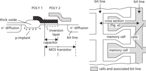
(a) Cross section of memory cell (not to scale) (b) Schematic top section showing memory cell packing
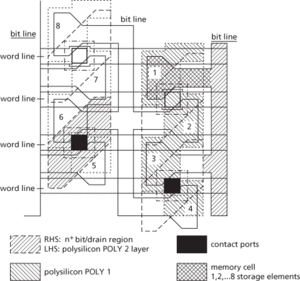
(c) Schematic top section of 8 bit section of MOSRAM memory
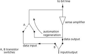
(d) Read-write circuit
A memory chip contains various logic circuits in addition to the memory cells and sense amplifiers: address decoders select the desired location; automatic refresh circuits regenerate the data; clocking circuits control the various functions and operate the switch transistors in order to perform read or write operations.
Static memories are used as cache memory in computer systems that require extremely high speeds of operation. They usually consist of an array of flip-flops connected to the address lines. A typical memory cell is shown in Fig. e for both bipolar and MOS circuits. In the latter case extra MOSFETs may be used as the load resistors. A high logic level (logical 1) at points A causes the transistors T2 to be ‘on’ and the voltage at points B therefore drops. This in turn causes transistors T1 to be ‘off’, which maintains the high voltage level at points A and the circuit is latched in that state. A low logic level at points A causes the reverse situation and transistors T1 are ‘on’. Power is continuously dissipated since one or other of the transistors is always conducting. The data is read using sense amplifiers connected to the bit lines.
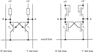
(e) Basic static memory cell