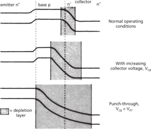
A type of breakdown that can occur in both bipolar junction transistors and field-effect transistors. If the collector-base voltage, VCB, applied to a bipolar junction transistor is increased, the depletion layer associated with the collector-base junction spreads across the base region. At a sufficiently high collector voltage, known as the punch-through voltage, VPT, the depletion layer spreads through the entire base region and reaches the emitter junction. A direct conducting path is therefore formed from emitter to collector and charge carriers from the emitter ‘punch through’ to the collector. The associated energy diagram is shown in Fig. a.

(a) Punch-through: energy diagrams for an n-p-n transistor at different collector voltages
In a field-effect transistor the effect operates in a similar manner. When the drain voltage, VD, reaches a sufficiently large value (VPT) the depletion layer associated with the drain spreads across the substrate and reaches the source. Charge carriers then punch through the substrate.
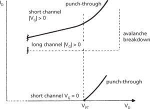
Punch-through can be a problem in a short-channel device used as a switch. Due to the relatively high doping level of the drain of an FET the drain-substrate depletion layer spreads readily across the substrate. Punch-through therefore must be avoided in the ‘off’ state of the switch, when the gate voltage, VG, is zero. Punch-through can also occur in the ‘on’ state (|VG| > 0) when the device is operated in the saturated region above pinch-off (see field-effect transistor); charge carriers punch through the substrate from source to drain at sufficiently large values of VD. In FETs that have relatively long channel lengths and high doping levels, punch-through does not occur; avalanche breakdown occurs first (Fig. b).

(b) FET characteristics above pinch-off
- random sampling
- random variable
- random variation
- random vector
- random walk
- random zero
- Raney nickel
- range
- range chart
- range finding
- range image
- range(in mechanics)
- range(in statistics)
- Firewire
- fireworks mode
- FIR filter
- firing
- firing room
- firing rule
- firm
- firm decision decoding
- Firmicutes
- firm objective
- firm-specific human capital
- firmware