A form of microscope that uses a beam of electrons instead of a beam of light (as in the optical microscope) to form a large image of a very small object. In optical microscopes the resolution is limited by the wavelength of the light. High-energy electrons, however, can be associated with a considerably shorter wavelength than light; for example, electrons accelerated to an energy of 105 electronvolts have a wavelength of 0.004 nanometre (see de Broglie wavelength) enabling a resolution of 0.2–0.5 nm to be achieved. The transmission electron microscope has an electron beam, sharply focused by electron lenses, passing through a very thin metallized specimen (less than 50 nanometres thick) onto a fluorescent screen, where a visual image is formed. This image can be photographed. The scanning electron microscope can be used with thicker specimens and forms a perspective image, although the resolution and magnification are lower. In this type of instrument a beam of primary electrons scans the specimen and those that are reflected, together with any secondary electrons emitted, are collected. This current is used to modulate a separate electron beam in a TV monitor, which scans the screen at the same frequency, consequently building up a picture of the specimen. The resolution is limited to about 10–20 nm.

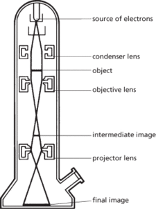
Electron microscope. Principle of transmission electron microscope.
http://micro.magnet.fsu.edu/primer/java/electronmicroscopy/magnify1/index.html A tutorial featuring virtual scanning electron microscopy, created by the Optical Microscopy Division of the National High Magnetic Field Laboratory
A form of microscope that uses a beam of electrons instead of a beam of light (as in the optical microscope) to form a large image of a very small object. In optical microscopes the resolution is limited by the wavelength of the light. High-energy electrons, however, can be associated with a considerably shorter wavelength than light; for example, electrons accelerated to an energy of 105 electronvolts have a wavelength of 0.004 nanometre (see de Broglie wavelength) enabling a resolution of 0.2–0.5 nm to be achieved. The transmission electron microscope has an electron beam, sharply focused by electron lenses, passing through a very thin metallized specimen (less than 50 nanometres thick) onto a fluorescent screen, where a visual image is formed. This image can be photographed. The scanning electron microscope can be used with thicker specimens and forms a perspective image, although the resolution and magnification are lower. In this type of instrument a beam of primary electrons scans the specimen and those that are reflected, together with any secondary electrons emitted, are collected. This current is used to modulate a separate electron beam in a TV monitor, which scans the screen at the same frequency, consequently building up a picture of the specimen. The resolution is limited to about 10–20 nm.
An instrument that uses a beam of electrons to investigate a sample in order to achieve a higher magnification and resolution than is possible with an optical microscope.
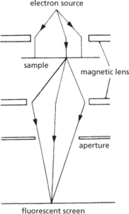
In the transmission electron microscope (TEM) the electron beam is focused by an electromagnetic lens or sometimes an electrostatic lens and has an energy of 50–100 kilovolts (Fig. a). A sharply focused image in one plane can only be obtained by using monoenergetic electrons. To avoid energy losses in the beam the sample must be extremely thin (<50 nanometres) so that the scattered electrons that form the image are not changed in energy, and the image therefore appears two-dimensional. A resolution of 0.2–0.5 nanometres is possible.
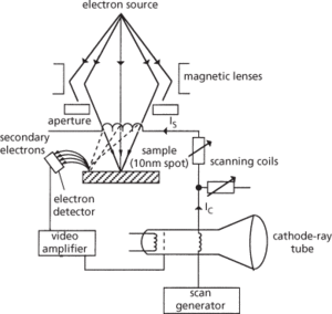
The scanning electron microscope (SEM) has lower resolution and magnification but produces a seemingly three-dimensional image, with great depth of field, from a sample of any convenient size or thickness (Fig. b). The sample is scanned by the electron beam, the numbers of resulting secondary electrons being proportional to the geometry and other properties of the sample. These electrons are converted, by means of an electron detector, scintillator, and photomultiplier, into a highly amplified signal that is used for intensity modulation of the beam of the display cathode-ray tube. The resolution is about 10–20 nm.
Different forms of these two types have been developed. The scanning-transmission electron microscope (STEM) combines the high resolution of the transmission instrument with the perspective image of the scanning type. The scanning-tunnelling microscope (STM) and the atomic force microscope (AFM) have even higher resolution, producing computer-generated contour maps of the sample surface. See scanning probe microscopy.

(a) Transmission electron microscope

(b) Scanning electron microscope
Both the TEM and the STEM can be used to produce diffraction patterns from thin samples of crystalline material such as semiconductors, rather than the usual image. This can be used to analyse the crystal structure of such materials. See also diffraction.
A form of microscope that uses a beam of electrons instead of a beam of light (as in the optical microscope) to form a large image of a very small object, such as a cell organelle, a virus, or a DNA molecule. In optical microscopes the resolution is limited by the wavelength of the light. High-energy electrons, however, can be associated with a considerably shorter wavelength than light; for example, electrons accelerated to an energy of 105 electronvolts have a wavelength of 0.04 nanometre, enabling a resolution of 0.2–0.5 nm to be achieved. The transmission electron microscope (see illustration) has an electron beam, sharply focused by electron lenses (coils producing a magnetic field or electrodes between which an electric field is created), passing through a very thin metallized specimen (less than 50 nanometres thick) onto a fluorescent screen, where a visual image is formed. This image can be photographed. High-resolution transmission electron microscopy (HRTEM), also called phase-contrast TEM, can achieve resolutions below 0.05° nm, enabling direct imaging of atomic structure. The scanning electron microscope can be used with thicker specimens and forms a perspective image, although the resolution and magnification are lower. It is used particularly for examining surface features of small objects, such as pollen grains. In this type of instrument a beam of primary electrons scans the specimen and those that are reflected, together with any secondary electrons emitted, are collected. This current is used to modulate a separate electron beam in a TV monitor, which scans the screen at the same frequency, consequently building up a picture of the specimen. The resolution is limited to about 10–20 nm. See also field-emission microscope; field-ionization microscope; immunoelectron microscopy.

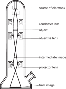
Principle of transmission electron microscope
http://micro.magnet.fsu.edu/primer/java/electronmicroscopy/magnify1/index.html Tutorial featuring virtual scanning electron microscopy, created by the Optical Microscopy Division of the National High Magnetic Field Laboratory
A microscope that uses beams of high-energy electrons rather than photons to form images. The momentum (p) of an electron depends on the voltage accelerating it, and the wavelength (λ) of the electron beam depends on the momentum of the electrons: λ = h/p, where h is Planck’s constant. A beam of high-energy electrons at 100 keV has a wavelength of approximately 3.7 pm, compared with the wavelength of about 500 nm for green visible light. Consequently, an electron beam is able to resolve details many times smaller than is possible with a light microscope. See scanning electron microscope; transmission electron microscope.
- recoverable error
- recovery
- recovery data
- recovery factor
- recovery log
- recovery point
- recovery rate
- recreation
- recreational drug
- recruitment
- recrystallization
- rectal gland
- rectangle
- rectangular
- rectangular cartogram
- rectangular coordinates
- rectangular distribution
- rectangular drainage
- rectangular hyperbola
- rectangular number
- rectangular pulse
- rectangular window
- rectification
- rectification section
- rectified spirit