MOS circuits or transistors that are fabricated using double diffusion. Regions of different conductivity type are formed by successive diffusion of different impurities through the same opening in the oxide layer. DMOS devices are short-channel high-performance devices that were originally developed for microwave applications. They have a very precise channel length that is determined by the double diffusion rather than the inherently less precise method of photolithography.
The speed of operation of a MOS transistor (or MOSFET) is determined by the channel length; for high operating speeds short channel lengths are required. Ordinary MOSFETs formed by a single diffusion (Fig. a) suffer from punch-through at short channel lengths since the depletion layer associated with the reverse-biased p-n+ drain junction spreads rapidly through the p-region as the drain voltage is increased. In the DMOS device an n– substrate is used. The p-regions are formed by diffusion (see planar process) followed by an n+ source/drain diffusion in which the source diffusion is made into the p-regions. An n+-p-n–-n+ structure is produced (Fig. b) in which an n– region, termed the drift region, separates the p-region from the n+ drain. The drain junction therefore becomes a reverse-biased p-n– junction and the associated depletion layer is almost entirely contained within the n-region.
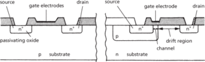
(a) Cross section of n-channel MOSFET (b) Cross section of n-channel DMOS transistor
The breakdown voltage of a DMOS device is determined by the width of the drift region up to a theoretical maximum determined by the characteristics of the n− semiconductor (see avalanche breakdown; depletion layer). High-voltage MOSFETs can be formed using relatively wide drift regions. Breakdown voltages up to 300 volts with drift regions of about 25 micrometres have been produced. Devices with relatively short drift regions are produced as integrated circuits for low-power high-speed (up to microwave frequency) applications.
Epitaxial DMOS transistors are formed in an n− epitaxial layer grown on a p-type substrate. Individual transistors on a chip may then be isolated by performing extra p-type isolating diffusions. See also VMOS.