A semiconductor diode used to detect the presence of light or to measure its intensity. It usually consists of a p–n junction device in a container that focuses any light in the environment close to the junction. The device is usually biased in reverse so that in the dark the current is small; when it is illuminated the current is proportional to the amount of light falling on it. See photoelectric cell; photoelectric effect.
A semiconductor p–n junction diode used to detect light or measure its intensity. The photodiode is encapsulated in a transparent plastic case that allows light to fall onto the junction. When this occurs, the reverse-bias resistance (high resistance in the opposite direction to normal current flow) drops and allows a larger reverse-biased current to flow through the device. The increase in current can then be related to the amount of light falling on the junction.
Photodiodes that can detect small changes in light level are used in alarm systems, camera exposure controls, and optical communication links.
A semiconductor diode that produces a significant photocurrent when illuminated. There are two main classes of photodiode: depletion-layer photodiodes and avalanche photodiodes.
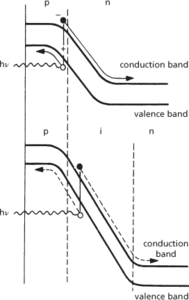
A common form of depletion-layer photodiode consists of a reverse-biased p-n junction operated below the breakdown voltage. When exposed to electromagnetic radiation of suitable frequency, excess charge carriers are produced as a result of photoconductivity; these carriers are in the form of electron-hole pairs. They usually recombine very quickly but those generated in or near the depletion layer present at the junction cross the junction and produce a photocurrent (Fig. a). The photocurrent is superimposed on the normally very small reverse saturation current, or dark current. The p-n junction can be formed by any of the usual methods and illumination can be either normal to the plane of the junction or parallel to it.

(a) Energy bands of reverse-biased p-n junction (top) and p-i-n photodiodes
The p-i-n (or PIN) photodiode (Figs. a, b) contains a layer of intrinsic (i-type) semiconductor material sandwiched between the p- and n-regions. The depletion layer is wholly contained within the i-region. The thickness of the intrinsic region can be adjusted to produce devices with optimum sensitivity and frequency response. The p-i-n photodiode is the most common type of depletion-layer photodiode.
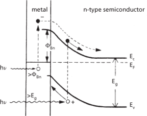
Depletion-layer photodiodes may also be realized using a metal-semiconductor junction, a heterojunction, or a point-contact diode. The Schottky photodiode (Fig. c) uses a metal-semiconductor junction. For optimal operation, in order to avoid losses due to absorption and reflection the metal film must be very thin (about 10 nanometres) and an antireflection coating must be used.
The photocurrent can be caused by two mechanisms, which depend on the value of the incident photon energy, hν, relative to the energy gap, Eg, of the semiconductor and the reduced work function, ΦBn, of the metal (Fig. d):
photoelectric emission of electrons from metal to semiconductor occurs;
photoconductive electron-hole pairs are produced in the semiconductor.
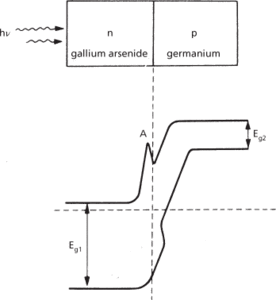
The heterojunction photodiode is formed from two semiconductors of different band gaps (Fig. e). The frequency response depends on the relative absorption of the two materials, suitable choice of material causing most of the radiation of a particular frequency to be absorbed close to the junction. Such diodes have a high speed of response and are highly frequency-selective. The small barrier, A, in the energy diagram is due to the discontinuity in the conduction bands and can be crossed by tunnelling (see tunnel effect) or surmounted by electrons with sufficiently high energy.

(b) A p-i-n photodiode (c) Schottky photodiode

(d) Simplified energy diagram for Schottky photodiode

(e) Heterojunction photodiode
Modulation of the intensity of illumination falling on a photodiode produces a modulated photocurrent that is dependent on the incident illumination.
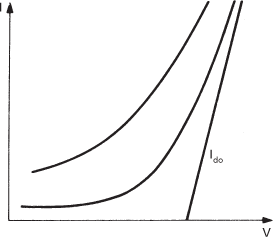
The other class of photodiodes, avalanche photodiodes, are reverse-biased p-n junction diodes that are operated at voltages above breakdown voltage. Current multiplication of electron-hole pairs, generated by the incident electromagnetic radiation, occurs due to the avalanche process. The photomultiplication factor, Mph, is defined as the ratio of the multiplied photocurrent, Iph, to the photocurrent, Ipho, at voltages below breakdown where no avalanche multiplication takes place. Static current-voltage characteristics are shown in Fig. f. The current I is the sum Iph + Ido, where Ido is) the dark current. The variation of Ido is also shown. The maximum photomultiplication depends inversely on the square root of Ido, and in order to achieve optimum operation Ido must be kept as small as possible. The device is thus operated with the voltage, V, approximately equal to the breakdown voltage, VB. Avalanche photodiodes provide a substantial gain at microwave frequencies. Schottky photodiodes may also be operated in the avalanche region.

(f) I–V characteristics of an avalanche photodiode
http://ecee.colorado.edu/~bart/book/book/chapter4/ch4_7.htm The basic principles of photodiodes
- mutarotation
- mutation
- mutation frequency
- mutation rate
- mutatis mutandis
- mutatus
- Mutesa I (1884)
- Mutesa II, Sir Edward Frederick (1924–69)
- muting
- muting switch
- Mutiny Act (1689)
- mutual branch
- mutual capacitance
- mutual exclusion
- mutual fund
- mutual inductance
- mutual-inductance coupling
- mutual information
- mutualism
- mutual knowledge
- mutually disjoint
- mutually exclusive
- mutually exclusive events
- mutually exclusive/jointly exhaustive
- mutually independent events