The creation of a solid using a chemical reaction in the vapour phase. First, the reactants are formed in the vapour state; this vapour is then transported to the desired location and deposited on a substrate. Many different types of solids can be prepared in a controlled manner using this method. For example, silicon and other semiconductors can be prepared using CVD.
A coating process that uses a reactant gas or vapour that decomposes onto the heated surface of a material depositing a solid element or compound. The process takes place in a chamber and the deposition forms coatings that are corrosion resistant and durable. CVD is used to provide coatings in the production of integrated circuits, anti-oxidation coatings of refractory materials, and hard cutting-tool coatings of titanium carbide, and other similar materials.
A technique for depositing thin films of metal, semiconductor, or insulator, employed in the manufacture of semiconductor devices and integrated circuits using planar process technology. The films are produced from gas-phase source materials that react on the surface of the sample to produce the film. A simple reactor is shown in the diagram: the heating can be provided directly, by radiant heaters, or by induction heating using a radiofrequency signal.
The deposition rate of the film is governed by the temperature of the sample and the pressure of the reactant gases inside the reactor. These parameters can also affect the quality of the resulting film, in terms of its chemical purity and number of defects present in the crystalline film. Metallic films are usually polycrystalline. Insulating films such as silicon dioxide or silicon nitride, used for isolation between metal layers or as capacitor dielectrics, are amorphous layers. Semiconductor layers can be deposited using CVD techniques: amorphous or polycrystalline films can be deposited, the crystalline order controlled by temperature with lower temperatures producing less-ordered films.
Epitaxial crystals can be grown on semiconductor surfaces using CVD techniques, the reactants and conditions chosen to enable the reaction at the semiconductor surface to produce a layer following the crystalline ordering of the underlying layer; this process is also known as vapour phase epitaxy (VPE). Often the reactants are inorganic materials, though recently the use of organic compounds containing metal atoms has been employed for VPE of compound semiconductors – this process being called organo-metallic vapour phase epitaxy (OMVPE).
Generally these reactions are carried out at reduced pressure, and the process is called low pressure chemical vapour deposition (LPCVD). Faster deposition occurs at higher pressures, and some processes can take place at atmospheric pressure: atmospheric pressure chemical vapour deposition (APCVD). Reaction rates can also be speeded up by using energetic reactant gases: the use of a glow discharge or plasma at low pressure to provide highly energetic and reactive species is employed in plasma-enhanced chemical vapour deposition (PECVD).
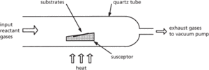
Reactor tube for chemical vapour deposition process
- disvalue
- dithered colour
- dithering
- dither noise
- dithionate
- dithionic acid
- dithionite
- dithionous acid
- Ditomopyge
- Dittmar’s law
- Dittus–Boelter correlation
- diuresis
- diuretic
- diurnal
- diurnal aberration
- diurnal inequality
- diurnal libration
- diurnal motion
- diurnal parallax
- diurnal rhythm
- diurnal temperature variation
- diurnal variation(geomagnetic)
- div
- divalent
- divariant assemblage