See integrated circuit.
A type of monolithic integrated circuit based on bipolar junction transistors. A section of a typical circuit is shown in the diagram. 1981 The substrate (E) is formed from a wafer of semiconductor (p-type is shown) and has buried n+ (highly doped) regions selectively diffused into it. These regions serve to reduce the collector series resistance of the completed transistors. The n-type epitaxial layer (D) is then grown on the substrate, and this in turn has an insulating oxide layer (B) grown on it. Photolithography is used to etch the oxide layer in the desired positions and isolating diffusions (C), of the same semiconductor type as the substrate, are made to isolate the individual components from each other. The individual components are formed by oxide growth, photolithography, etching, and diffusion of the appropriate type of impurity, in turn, into the epitaxial layer. A final passivating oxide layer is grown. This has windows etched into it to enable contacts to be made to the semiconductor; the desired interconnection pattern is made by evaporating a metal layer (A), usually aluminium, on to the oxide and etching.
The substrate is held at the most negative potential possible, thus causing the collector-substrate junctions to be reverse biased and preventing current flow across them. This ensures isolation of the individual components. The n-type region surrounding the resistor – the resistor box – is held at the most positive potential possible, thus preventing current flow across the resistor-resistor box junction by ensuring that it too is reverse biased.
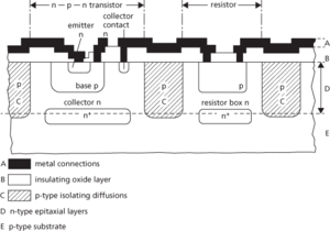
Cross section of typical bipolar integrated circuit
- Svedberg unit
- SVG
- SVGA
- SVN
- Svobodny
- Kirov, Sergei Mironovich (1886–1934)
- Kirpichev number
- Kishi Nobusuke (1896–1987)
- Kissinger, Henry Alfred (1923–)
- Kistiakowsky, George Bogdan
- Kita Ikki (1937)
- Kitasato, Baron Shibasaburo
- kitchen cabinet
- Kitchener, Herbert, 1st Earl Kitchener of Khartoum (1850–1916)
- kite
- Kitt Peak National Observatory
- Kizim, Leonid (1941–2010)
- Kjeldahl, Johan Gustav Christoffer Thorsager
- Kjeldahl’s method
- KK-thesis
- kLa
- Klaproth, Martin Heinrich
- Klatt synthesizer
- Klazminskian
- Kleene closure