A family of bipolar integrated logic circuits that are very compact and provide a very high functional packing density combined with the possibility of high-speed operation. I2L is essentially a development derived from diode transistor logic (DTL). The input diodes and transistors of DTL are combined in I2L into a single multicollector n-p-n transistor, and the current source is provided by a p-n-p transistor rather than a load resistor. The p-n-p transistor is formed in the same area of chip as parts of the multicollector transistor allowing a very compact structure. The multicollector structure provides the isolation between logic gates provided in DTL by the input diodes of the following gates.
A typical structure is shown in Fig. a and the equivalent circuit in Fig. b. The p-n-p transistor is arranged laterally on the chip; the p-type emitter is common to a large number of gates and is termed the injector. The n-p-n transistor is a vertical transistor, which is inverted compared to the usual method of fabrication. The n-type epitaxial layer forms the base of the p-n-p transistor and the emitter of the n-p-n transistor and is common to all the gates. An n+ guard ring surrounds each p-type p-n-p collector/n-p-n base region containing the n+ n-p-n collectors, in order to provide isolation between individual gates. The fan-out is determined by the number of multiple collectors.
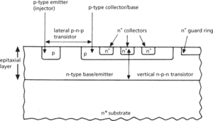
(a) Cross section of I2L gate
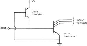
(b) Equivalent circuit of single I2L gate
A basic 3-input NOR gate is shown in Fig. c. If any of the collectors of gates 1, 2, or 3 is at the low logic level, current from the p-n-p transistor flows to that collector (indicated by the dashed line) and the transistor T4 is ‘off’. The collectors of T4 are therefore at the high logic level. If all the inputs are high T4 is ‘on’ and current from the p-n-p transistor flows through T4 and the collector voltages are low. The p-n-p transistors are not shown but are indicated by the label ‘injection current’.
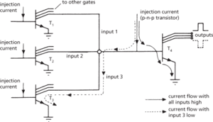
(c) Basic NOR gate
The difference between the high and low logic levels is determined by the forward voltage of the base-emitter junction of the multicollector transistor and the circuits can operate with a total voltage swing of about 0.7 volts. The power consumed by the circuits is a linear function of the speed at which they are operated and the circuits can be designed to optimize the speed and power at any point within the circuit. The small voltage change renders the I2L circuit susceptible to stray noise pulses or interference when used alone, and on-chip input and output buffer circuits are normally used to convert pulses from transistor-transistor logic to those suitable for I2L and vice versa.
Schottky I2L is a form of I2L in which the collectors are formed as Schottky diodes. Excessive carrier storage at the collector junction is reduced and the speed of operation is therefore increased. The total voltage swing is also reduced due to the characteristically small forward voltage of the Schottky diode. The speed of operation of the Schottky I2L circuits may also be increased using Schottky diodes across the base-collector junction to prevent the output transistors from going too far into the saturated mode, and hence keeping charge-storage times to a minimum.
I2L has found many varied applications. It is fabricated using standard bipolar techniques and other types of circuit, such as LED drivers, operational amplifiers, and oscillators, can be easily produced on the same chip allowing great flexibility.
- Hammett equation
- Hamming bound
- Hamming code
- Hamming codes
- Hamming distance
- Hamming metric
- Hamming radius
- Hamming, Richard Wesley (1915–98)
- Hamming space
- Hamming sphere
- Hamming weight
- Hamming window
- Hammond, (Lloyd) Blaine, Jr (1952– )
- Hammond’s postulate
- Hammurabi (1750)
- Hampden, John (1594–1643)
- Hampton Court Conference (1604)
- Hampton Roads Conference (3 February 1865)
- ham radio
- hamster
- Han
- Hancock, John (1737–93)
- hand controller
- hand geometry biometrics
- hand-held computer