A PGA that may be programmed by the user, i.e. on the customer’s premises. See also programmed logic.
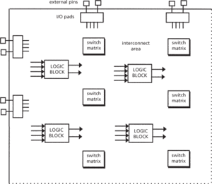
(field programmable gate array) An array of logic cells placed in an infrastructure of interconnections, where each logic cell is a universal function – a functionally complete logic device – that can be programmed to realize a certain function. Interconnections between cells are also programmable, but unlike other programmable logic devices (PLDs) these interconnections are of different types and several paths are possible between two given points in the circuit (Fig. a); all prediction of the timing is impossible before the final routing of the circuit. Input/output cells are equally programmable, but with fewer possibilities (direction of the information, storage element, electrical level) than logic cells.

(a) Corner of a typical FPGA
The complexity of the internal logic of an FPGA renders it comparable to a gate array, and its cycle of design is also very similar. Its main advantage is the time of realization: programmable on the spot, an FPGA circuit is in a working state a few minutes after the end of the design, compared to some months for a gate array.
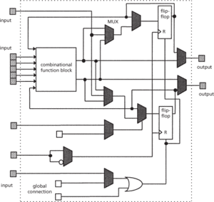
One of the differences between FPGAs and other programmable devices is that one FPGA logic block can be programmed to implement a two- to four-level combinational logic circuit, and the output(s) of that logic block can become the inputs to other logic blocks. An example of the lower-level logic block is shown in Fig. b, where there are two flip-flops, nine multiplexers, and a seven-input combinational function unit. The combinational unit can be programmed to realize any two four-input logic functions, or any one five-input logic function (similar to an embedded PLA). The logic block accommodates up to eight inputs and two outputs.

(b) Logic cell for typical FPGA
- metal spraying
- metaluminous
- metal–insulator transition
- metamagnet
- metamale
- metamaterial
- metamathematics
- metameric segmentation
- metamerism
- metamict state
- metamorphic aureole
- metamorphic differentiation
- metamorphic facies
- metamorphic grade
- metamorphic rock
- metamorphic rock classification
- metamorphic zone
- metamorphism
- metamorphosis
- metanephridium
- metapelite
- metaphase
- metaphilosophy
- metaphloem
- metaphor