See transistor.
A semiconductor device having three terminals: source, gate, and drain. Current flow in a narrow conduction channel between drain and source is controlled by the voltage applied between gate and source, which can deplete the conduction channel of charge carriers. If the source and drain regions are composed of n-type semiconductor the conduction channel is n-type; these devices are known as n-channel devices. Devices with p-type source, drain, and channel are called p-channel devices. In contrast to bipolar transistors, FETs are unipolar devices; the current flow is electrons (in n-channel devices) or holes (in p-channel devices).
In the junction FET the channel is a composite part of the structure. In the MOSFET the gate is insulated from the source and drain regions and the channel forms when the gate voltage is applied. Unlike the bipolar transistor both types of FET require virtually no input current to the gate except a pulse to charge or discharge the gate capacitance. Junction FETs have relatively slow switching speeds compared with MOSFETs and bipolar transistors, and are therefore not used in logic circuits. FETs appear in vast numbers in microprocessor chips and similar devices.
One of the two major classes of transistor. It is a three-terminal semiconductor device in which the current flow through one pair of terminals, the source and the drain, is controlled or modulated by an electric field that penetrates the semiconductor; this field is introduced by the voltage applied at the third terminal, the gate (Fig. a). The resistance of the channel is controlled by the field, producing a voltage-controlled resistor.
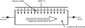
(a) Field-effect transistor operation
The controlling field is applied to the gate electrode, but must be isolated somehow from the current flow in the channel. The method of isolation yields two basic types of field-effect transistor: the junction field-effect transistor (JFET) and the insulated-gate field-effect transistor (IGFET). In JFETs the isolation is provided by a reverse-biased p-n junction or a metal-semiconductor Schottky barrier, so the current flow across the junction from gate to channel is very small (see also MESFET). In IGFETs an insulating layer is placed between the gate electrode and the conducting channel, preventing any current flow between them. The most widely known practical example of the insulated-gate FET is the MOSFET (metal-oxide-silicon FET).
The conducting channel in JFETs is in the body of the semiconductor, and these transistors are classed as bulk-channel FETs. In MOSFETs the conducting channel lies at the surface of the silicon, at the silicon-oxide interface; these transistors are surface-channel FETs.
The FETs are generally described by the type of charge carrier that conducts the current in the channel: there are therefore p-channel FETs, where holes provide the conduction, and n-channel FETs, where electrons conduct. FETs can be further described by the nature of the channel: depletion-mode FETs have the conducting channel already present at zero gate voltage, and an appropriate voltage must be applied to close the channel, or turn off the FET; enhancement-mode FETs have no conducting path present between source and drain at zero gate voltage, and an appropriate gate voltage must be applied to open the channel. The voltage at which the channel is just becoming conducting is known as the threshold voltage, VT. The presence or absence of the channel at zero volts gate voltage is determined by the details of the doping of the channel region of the FET. The general variation of drain current ID with applied gate voltage VG for the various types of FET is shown in Fig. b.
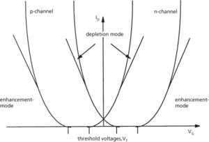
(b) Drain-current/gate-voltage relationships for FETs
The output characteristics of an n-channel FET are shown in Fig. c. These curves show the linear or triode region of operation at low values of drain-source voltage VDS, corresponding to the voltage-controlled resistance described above, and the saturation region at higher values of VDS. In the saturation region the FET channel is restricted in width, and the current flow cannot increase with further increases in the channel voltage VDS. The FET behaves like a voltage-controlled current source. This is the region of operation for linear amplification applications. For digital switching applications, such as logic, the FET is switched between the ‘off’ state, below threshold, to a high-current ‘on’ state in the triode region.
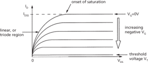
(c) n-channel FET output (drain-current/drain-source voltage) characteristics
- Homunculus Nebula
- Honda–Mrkos–Pajdusakova
- Honduras
- Honecker, Erich (1912–94)
- honestly significant difference test
- honeycomb coil
- honeycomb weathering
- honeynet
- honey pot
- honey-pot
- honeysuckle
- Hong Kong Statistical Society
- Hong Kong Stock Exchange
- HOOD
- Hood, Leroy Edward
- hoodoo
- Hood, Samuel, 1st Viscount (1724–1816)
- Hooke, Robert
- Hooke, Robert (1635–1703)
- Hooker, Richard (1554–1600)
- Hooker, Sir Joseph Dalton
- Hooker Telescope
- Hooker, William Jackson
- Hooker–Raschig process
- Hooke–Jeeves pattern search