A set of integrated logic circuits. The input part of an ECL consists of an emitter-coupled transistor pair which is a very good differential amplifier. The output is through an emitter follower. ECL circuits are very rapid logic circuits.
See ECL.
A family of integrated logic circuits so called because a pair of transistors coupled by their emitters forms a fundamental part of the circuit. The basic ECL gate has simultaneously the function required and its complement.
A simple OR/NOR circuit is shown in Fig. a. Input is via the bipolar junction transistors T1a,b,c; these are emitter-coupled to transistor T2 and form a long-tailed pair with it. This is an excellent differential amplifier. An emitter-follower buffer forms the output stage. Transistor T2 has a fixed bias applied to its base with magnitude halfway between a logical 1 and a logical 0. If a logical 0 is applied to all three input transistors then current flows through T2 causing a voltage drop across R2. This in turn produces a logical 0 at the OR output and a logical 1 at the NOR output. If any one of the input transistors T1a,b,c has a logical 1 applied, current flows through that transistor producing a voltage drop across R1 and the outputs are hence reversed, i.e. a logical 1 occurs at the OR output. Typical values of applied voltages are −1.55 volts (logical 0), −0.75 volts (logical 1), −1.15 volts (fixed bias).
The transistors are operated in nonsaturated mode and the delay is exceedingly short (approximately one nanosecond) making ECL circuits inherently the fastest type of logic circuit.
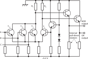
(a) ECL OR/NOR circuit
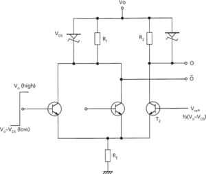
(b) Low-voltage ECL gate
Simpler versions of the original ECL circuits have been designed for VLSI circuits; these have a higher packing density and operate with lower voltage swings. Fig. b shows a simple low-voltage ECL gate in which the emitter-follower transistors are replaced by Schottky clamped-load resistors R1 and R2. The fixed reference bias applied to transistor T2 is generated ‘on-chip’ rather than being supplied externally. The total difference between the ‘high’ and ‘low’ logic levels is equal to the forward bias of the Schottky diode, VDS.
An alternative form of higher packing density ECL circuit uses ECL circuits connected in series (gated); this allows a more complex logic function to be implanted on a smaller area of chip. This method of series-gated circuit design is also widely used in FET circuitry.
- tobit analysis
- Tobit model
- Tobler’s first law of geography
- Tobruk, Siege of (1941–42)
- Toby Jug Nebula
- tocopherol
- Tocqueville, Alexis, Comte de (1805–59)
- Todaro model
- Todd, Alexander Robertus, Baron
- TOE
- Toeplitz matrix
- toeset
- locomotive
- locomotive principle
- locule
- locus
- locutionary act
- lode
- lodestone
- lodgement
- lodgement till
- Lodge, Sir Oliver Joseph
- Lodge, Sir Oliver Joseph (1851–1940)
- Lodi
- lodicule