The most commonly used method of producing junctions during the manufacture of semiconductor devices. All the semiconductor devices are formed at the same time on one side of a semiconductor wafer. The device and IC structure is then planar rather than bulk three-dimensional. A layer of silicon dioxide is thermally grown on the surface of a silicon substrate of the desired conductivity type. Photolithography is used to etch holes in the oxide layer, which then acts as a mask for the diffusion of suitable impurities into the substrate in order to produce a region of opposite polarity. The junction between the two semiconductor types actually meets the surface of the substrate below the oxide since the diffusion occurs in directions both normal to and parallel to the surface of the silicon (Fig. a).
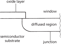
(a) Planar process
Several diffusions can be carried out serially. Usually a final layer of oxide is grown to cover the entire chip (except for the contacts) in order to provide a stable surface for the silicon and to minimize surface-leakage effects. The characteristics of early junction transistors tended to be dominated by surface-leakage effects and the planar process proved to be one of the most important single advances in semiconductor technology. A planar transistor is shown in Fig. b.
The n-p-n planar epitaxial transistor shown in Fig. c is a transistor formed by a combination of epitaxy and diffusion. The lightly doped epitaxial layer is grown on to the highly doped substrate and the junctions are formed by diffusion into the epitaxial layer. In this technique the highly doped substrate forms the bulk of the collector and the collector series resistance is therefore reduced while the lightly doped epitaxial layer maintains the collector-base breakdown characteristics.
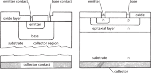
(b) Planar transistor (c) Planar epitaxial transistor
http://nobelprize.org/nobel_prizes/physics/articles/lecuyer/planar.html Jean Hoerni’s development of the planar process, on the Nobel Prize website
- Temple, William (1881–1944)
- Temple–Tuttle
- temporal cohesion
- Temporal Experiment for Storms and Tropical Systems Technology – Demonstration
- temporality
- temporal logic
- temporal stage
- temporal summation
- Temporary Assistance to Needy Families
- temporary equilibrium
- temporary file
- temporary hardness
- temporary magnetism
- temporary refuge
- TEM wave
- tenacity
- tender
- tender- and tough-minded
- tender issue
- tendon
- tendril
- tend to
- Tenma
- ten-minute hold
- tennantite