See photoelectric effect.
An effect arising when a junction between two dissimilar materials, such as a metal and a semiconductor or two opposite polarity semiconductors, is exposed to electromagnetic radiation, usually in the range near-ultraviolet to infrared. A forward voltage appears across the illuminated junction and power can be delivered from it to an external circuit. The effect results from the depletion region and resulting potential barrier invariably associated with an unbiased junction (see also p-n junction; metal-semiconductor contact).
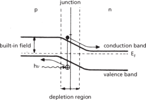
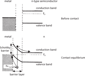
The energy bands are shown for a p-n junction and a metal-semiconductor contact (Figs. a, b overleaf). The incident radiation imparts energy to electrons in the valence band and electron-hole pairs are produced in the depletion region around the p-n junction or in the barrier layer at the metal-semiconductor contact. As the electron-hole pairs are produced they cross the junction due to the inherent field (Figs. a, b) and produce the forward bias: an excess of holes migrating into the p-type semiconductor or the metal produces a positive bias; electrons migrating into the n-type semiconductor produces a negative bias.
The photovoltaic effect is utilized in photovoltaic cells, such as solar cells.

(a) Photovoltaic effect

(b) Photovoltaic effect in metal-semiconductor contact
- cascade process
- Cascade SmallSat and Ionospheric Polar Explorer
- cascade tax
- cascading style sheets
- cascading system
- cascading systems
- cascode connection
- CASE
- case
- case-based reasoning
- case-controlled study
- case control studies
- case grammar
- case hardening
- casein
- casement plot
- Casement, Roger David (1864–1916)
- case-sensitive
- case statement
- Casey, Richard Gardiner, Baron (1890–1976)
- cash
- cash cropping
- cash discount
- cash flow
- cashless economy