A technique used in the manufacture of semiconductor components, integrated circuits, etc. It depends on the principle of masking selected areas of a surface and exposing the unmasked areas to such processes as the introduction of impurities, deposition of thin films, removal of material by etching, etc. The technique has been developed for use on tiny structures (typically measured in micrometres), which can only be examined by means of an electron microscope.
A technique used during the manufacture of integrated circuits, semiconductor components, thin-film circuits, and printed circuits. Photolithography is used in order to produce a desired pattern from a photographic mask – a photomask – on a substrate material preparatory to a particular processing step.
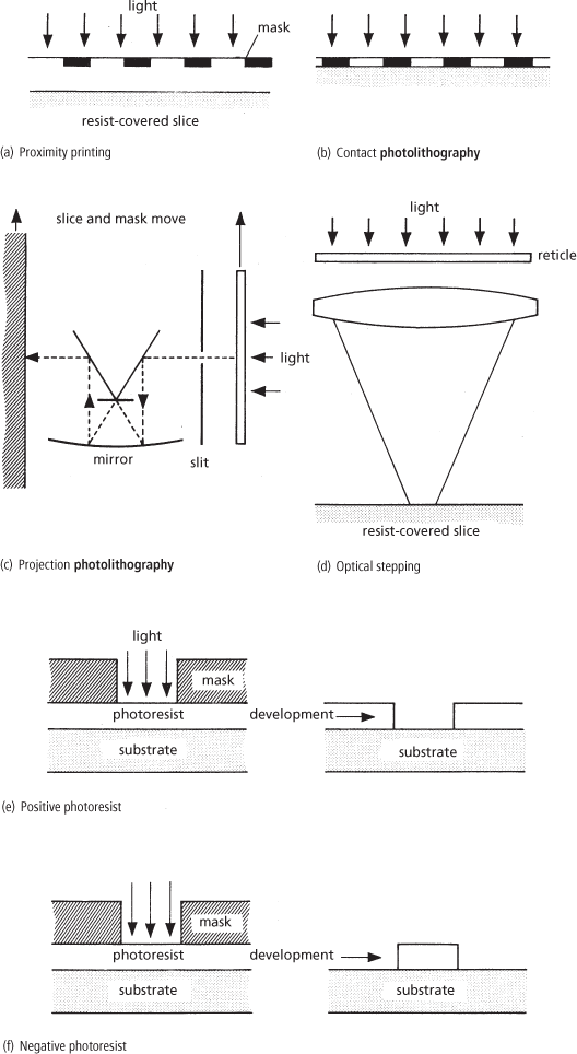
The clean substrate is covered with a solution of photoresist by spincoating, spraying, or immersion. The solution is allowed to dry and is then exposed to light or near ultraviolet radiation through the mask. Deep ultraviolet exposure can be used where greater resolution is required because of the shorter wavelength. Quartz masks rather than glass ones must then be used together with different resist material. The depolymerized portions of the photoresist are removed using a suitable solvent, and the polymerized portion remains and acts as a barrier to etching substances or as a mask for deposition processes. When the processing step is completed the remaining photoresist is removed using another suitable solvent.
Different methods are used to expose the resist through the mask. Proximity printing places the mask close to the slice but not in actual contact with it (Fig. a). The diffraction that occurs at the edges of the patterns on the mask causes divergence of the light and this method is only suitable for applications not requiring a high lateral resolution. Contact photolithography has the mask in contact with the surface of the slice. After alignment it is vacuum clamped to the slice for exposure (Fig. b). The resolution and uniformity of the technique depend critically on the mask being undamaged and the degree of contact that can be achieved. Any slight curvature of the slice or the mask causes runout, i.e. errors in the exposed pattern. The actual contact tends to damage the masks and they therefore have a limited life. Contact lithography however is a cheap and rapid technique and suitable for use with smaller slices and small-scale integrated circuits.
For large slices and VLSI circuits other methods are used. Projection photolithography uses an optical system to produce an image of the mask on the slice. The mask and slice are moved in synchronism to scan across the entire area (Fig. c). The depth of focus is very small and the slice therefore must have an extremely flat surface for accurate reproduction of the pattern. Optical stepping is the most commonly used technique for large-scale integration (LSI) applications, where good resolution and high yield are required. A mask, known as a reticle, contains the pattern for a portion of the slice (Fig. d). The pattern is imaged onto the slice, then the slice is moved and the exposure repeated. The step and repeat process continues until the entire slice has been exposed. The technique is particularly suitable for digital circuits where tens of thousands of identical devices are required. The pattern on the reticle can be up to ten times as large as the final pattern on the slice, allowing very accurate masks to be made. Optical steppers require extremely accurate optical systems and their complexity makes them very expensive.
All photolithographic techniques require excellent collimation of the light source, uniform and constant intensity over the whole of the mask area, and a vibration-free environment.
Positive photoresist is used to produce a positive image of the photographic mask. In this case the exposed portion is depolymerized and removed during development (Fig. e). Negative photoresist produces a negative image of the mask and it is the exposed portion that is polymerized and remains after development (Fig. f).
Photolithography is an important part of the planar process for the manufacture of integrated circuits. In the case of very complex integrated circuits the size of the components forming the circuits is nearly comparable to the wavelengths of the radiation used to produce the masks and large geometric errors can easily arise. Shorter wavelengths are therefore required and other lithography systems have been developed. See electron-beam lithography; ion-beam lithography; X-ray lithography.
- Slipher, Vesto Melvin
- Slipher, Vesto Melvin (1875–1969)
- slip-off slope
- slippage test
- slippery slope
- slip-plate
- slip ratio
- SLN
- Sloan Digital Sky Survey
- SLOC
- sloc
- slope
- slope angle
- slope modulation
- slope overload
- slope processes
- slope profile
- slope resistance
- slope stability
- slope stabilization
- slope wash
- slope winds
- slop oil
- slot antenna
- sloth